- 3 semiconductor layers
- NPN or PNP
- used as switch or amplifier
- different from just back to back diodes because there is interaction between the layers
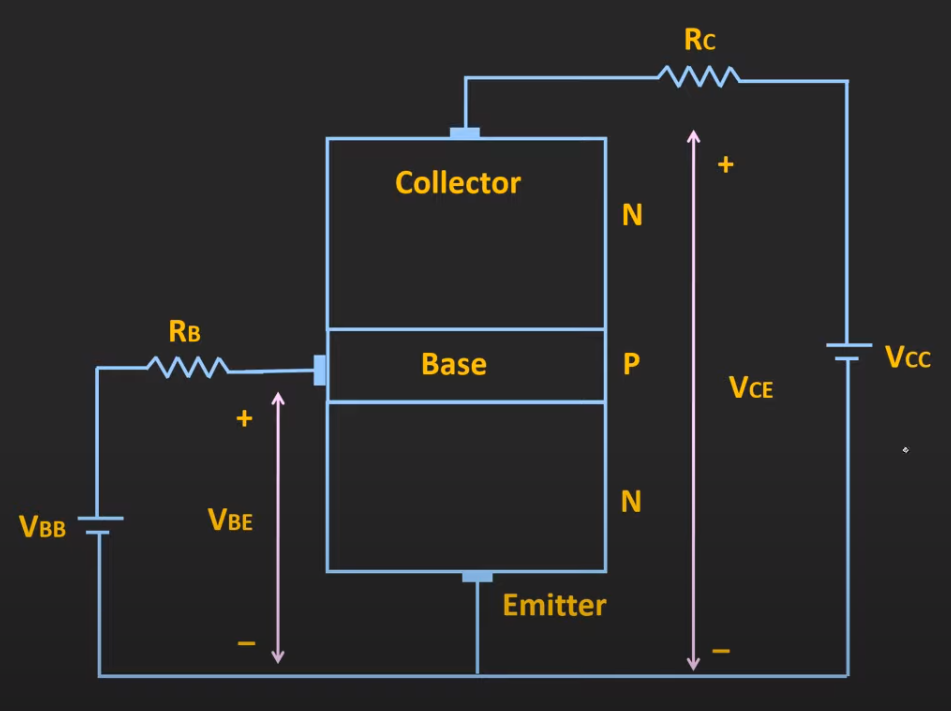
- is voltage at emitter, is voltage at the base, is the voltage at the collector
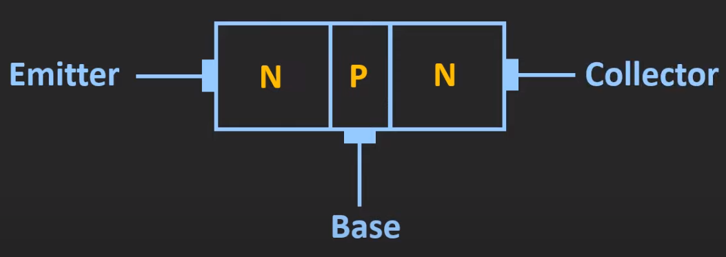
Layers
- emitter
- heavily doped (like conductor)
- base
- lightly doped (like insulator)
- very thin
- collector
- moderately doped (like semiconductor)
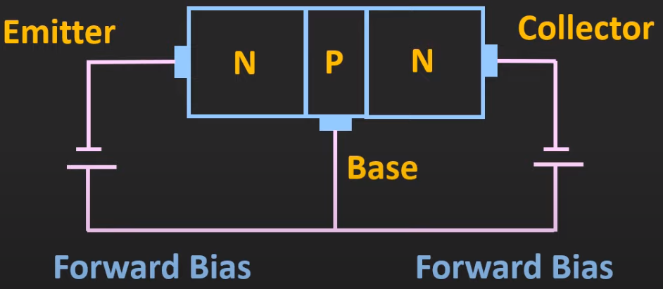
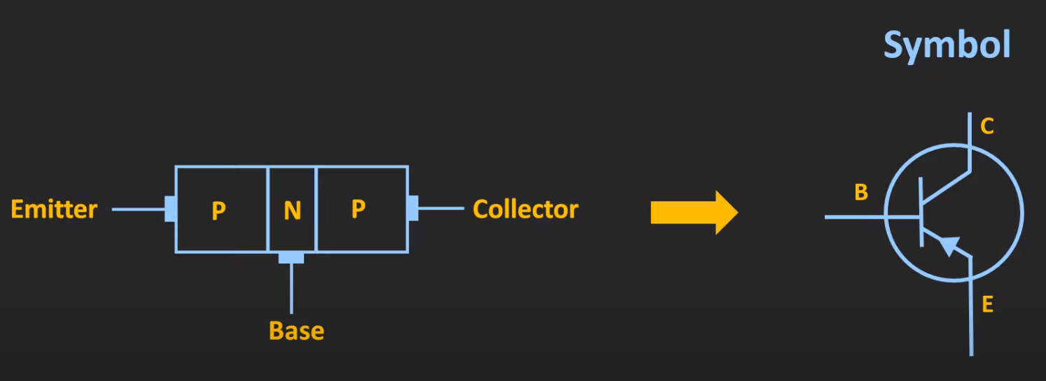
NPN
Diagram
Circuit Symbol
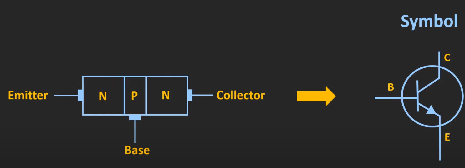
- arrow indicates the direction of current
Regions of Operation
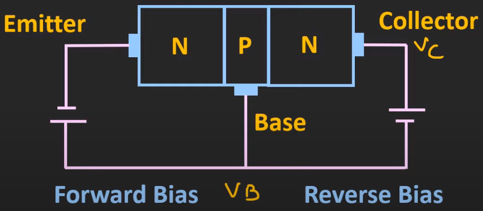
Active Region
- emitter is in forward bias
- collector is in reverse bias
- used for amplification
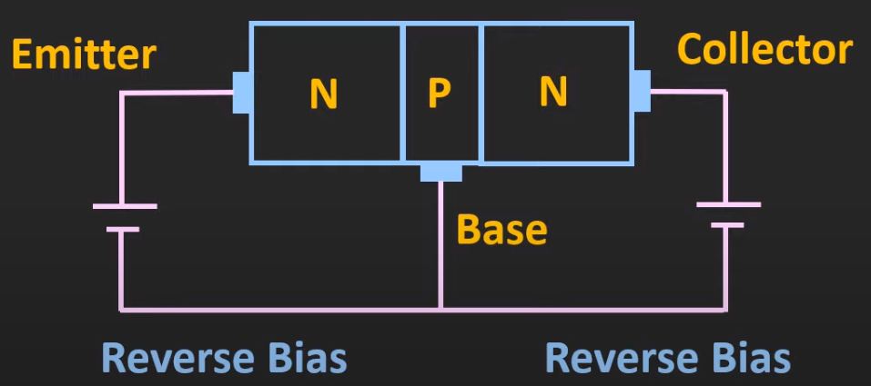
Cutoff Region
- emitter is in reverse bias
- collector is in reverse bias
- used for switching
Saturation Region
- emitter is in forward bias
- collector is in forward bias
- used for switching
Configurations
- different configurations are used for different applications
- 3 types
- common emitter
- current + voltage gain
- common base
- voltage gain but no current gain
- common collector
- current gain but no voltage gain
- “common” indicates that both of the other non-common component are connected to the common component
- example: common emitter means that both the base and collector are connected to the emitter
- common emitter
Transistor Working Demonstration
- let’s model a a NPN, common emitter BJT transistor working in the active region
- input is applied between the base and emitter
- output is measured between the collector and emitter.
- pushes electrons from the emitter to the base
- electrons in base have 2 options:
- flowing through and the positive terminal of
- flowing through and the positive terminal of
- most electrons flow to collector b/c
- collector is lightly doped
- base layer is very thin
In short, we just reiterated the Active Region section:
- current flows from emitter to base (emitter is forward biased)
- current flows from emitter to collector (reverse biased) (note that in the diagram in the Active Region section, current flows from base to collector because it’s a common base config)
Diagram of current:
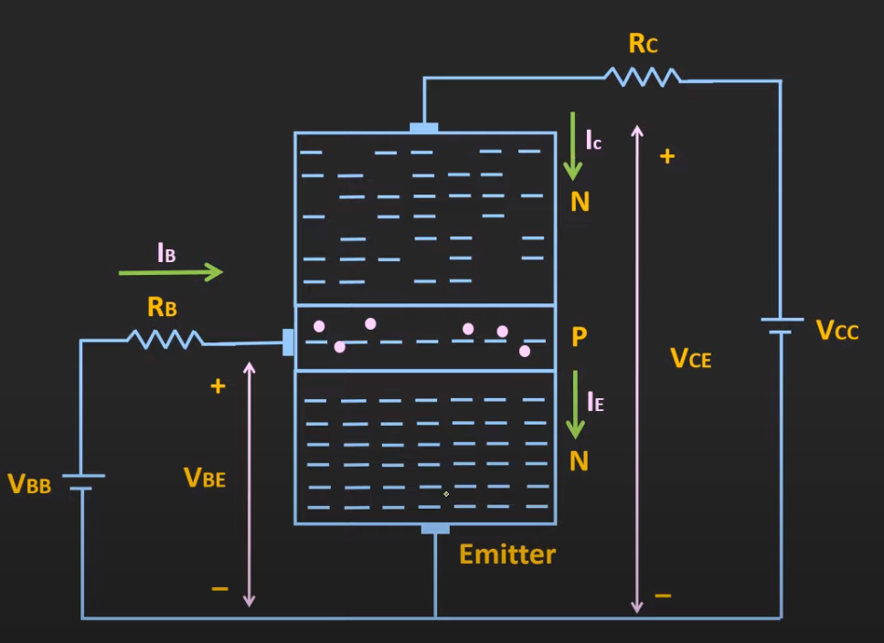
Now we perform KCL:
Since is the input and is the output, you can control the output () by just changing the base current.
PNP
Diagram
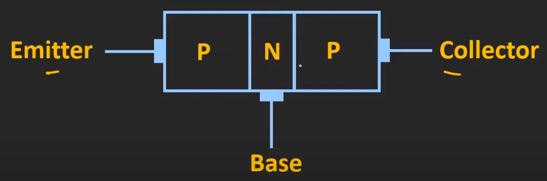
Circuit Symbol
- arrow indicates direction of current